Samsung Electronics Co., Ltd., a world leader in advanced semiconductor technology, today announced that its new cutting-edge semiconductor fabrication line in Hwaseong, Korea, has begun mass production.
This press release features multimedia. View the full release here: https://www.businesswire.com/news/home/20200220005359/en/
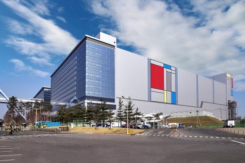
Samsung's new EUV Line in Hwaseong, Korea (Photo: Business Wire)
The facility, V1, is Samsung’s first semiconductor production line dedicated to the extreme ultraviolet (EUV) lithography technology and produces chips using process node of 7 nanometer (nm) and below. The V1 line broke ground in February 2018, and began test wafer production in the second half of 2019. Its first products will be delivered to customers in the first quarter.
"Along with technology leadership and design infrastructure, manufacturing excellence is one of the most important elements of the foundry business,” said Dr. ES Jung, President and Head of Foundry Business at Samsung Electronics. "As we ramp up production, the V1 line will enhance our ability to respond to market demand and expand opportunities to support our customers."
The V1 line is currently producing state-of-the-art mobile chips with 7 and 6nm process technology and will continue to adopt finer circuitry up to the 3nm process node.
By the end of 2020, the cumulative total investment in the V1 line will reach USD 6 billion in accordance with Samsung’s plan and the total capacity from 7nm and below process node is expected to triple from that of 2019. Together with the S3 line, the V1 line is expected to play a pivotal role in responding to fast-growing global market demand for single-digit node foundry technologies.
As semiconductor geometries grow smaller, the adoption of EUV lithography technology has become increasingly important, as it enables scaling down of complex patterns on wafers and provides an optimal choice for next-generation applications such as 5G, AI, and Automotive.
With the V1 line in operation, Samsung now has a total of six foundry production lines in South Korea and the United States, including five 12-inch lines and one 8-inch line. (see below)
* Global manufacturing sites of Samsung foundry
|
Name |
6-Line |
S1-Line |
S2-Line |
S3-Line |
S4-Line |
V1-Line |
|
Nodes |
180~65nm |
65~8nm |
65~11nm |
10nm~ |
65nm~ |
7nm~ |
|
Location |
Giheung, Korea |
Austin, USA |
Hwaseong, Korea |
|||
|
Wafer Size |
8-inch |
12-inch |
||||
# # #
About Samsung Electronics Co., Ltd.
Samsung inspires the world and shapes the future with transformative ideas and technologies. The company is redefining the worlds of TVs, smartphones, wearable devices, tablets, digital appliances, network systems, and memory, system LSI, foundry and LED solutions. For the latest news, please visit the Samsung Newsroom at http://news.samsung.com.
View source version on businesswire.com: https://www.businesswire.com/news/home/20200220005359/en/
Ujeong Jahnke
Samsung Semiconductor Europe GmbH
Tel. +49(0)6196-66-3300
Email: ujeong.j@samsung.com
Permalink: http://www.businesswire.com/news/home/20200220005359/en